Dynamic RAM (DRAM) must be periodically refreshed to maintain its content. If any bit is inadvertently swapped, we can say that the memory doesn’t work as it should. JEDEC (Joint Electron Device Engineering Council, a body that provides DDR specification, among other things) specifies how often this has to be done to ensure proper operation. However, some people are more interested in how long the data may be preserved after DRAM is powered down. In this blog post, we will describe how this can be measured, and what results we managed to get on a couple of tested platforms.
Some theory
RAM (Random-Access Memory) is a type of memory that can be accessed at random locations with little to no difference in time between different addresses. In this document, this term will be used to represent operating system’s view of memory as one(*) consecutive range of addresses.
DRAM (Dynamic RAM) is a type of RAM that holds the data in capacitors, which loses its charge over time and must be periodically refreshed. This is in contrast to static RAM (SRAM) which doesn’t require refreshing to hold its data. The capacitor, together with logic required to access its content, is called a DRAM cell. Multiple cells form a grid that is addressable by row and column, such grid is called a bank. Each bank (in most commonly available DRAM chips) is replicated 4 or 8 times in parallel, so each row/column pair addresses 4 or 8 bits of data per DRAM at once. On top of that, each DRAM can have multiple banks, addressed by bank group and bank address bits (up to 2 bits for each in DDR4).
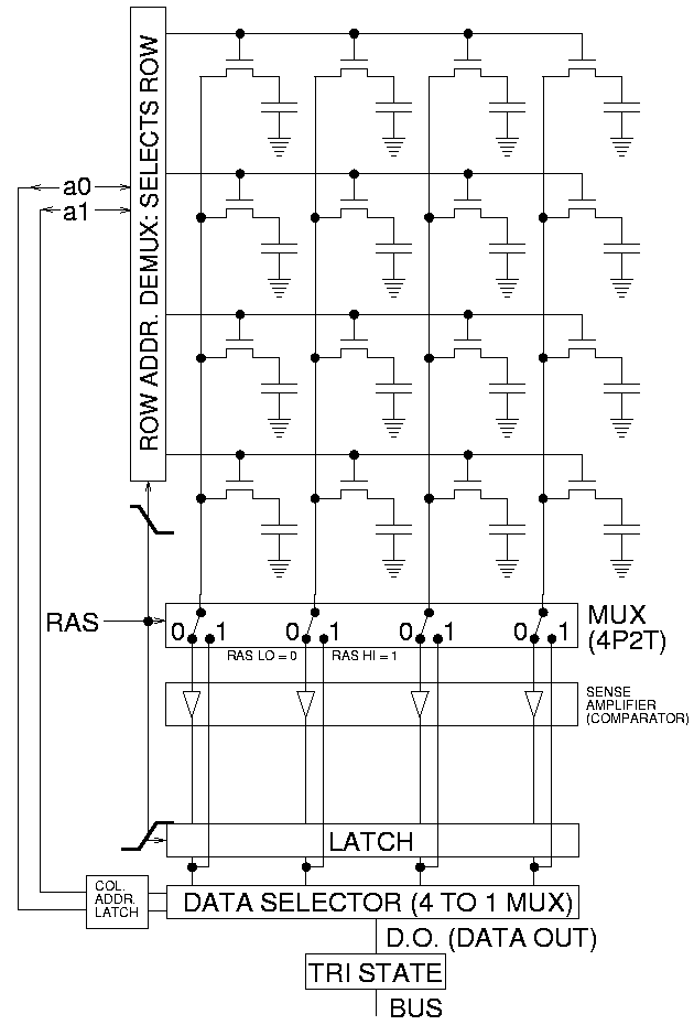
Simple DRAM grid with 2 row bits and 2 column bits
DIMM (Dual In-Line Memory Module) is a module that is most commonly associated with terms like “RAM module” or “memory stick”. It is installed in slots on mainboard, can be easily exchanged without using specialized tools. DIMMs consist of multiple of 8 (or 9 with ECC) DRAMs, all of which share row, column and bank addressing. In case of higher number of DRAMs, they are enabled in groups by chip select signals; this is arbitrated by DIMM based on rank address requested by the platform. All DRAM data lines are lined in parallel to form 64-bit wide (72-bit with ECC) DIMM data bus.
Mapping of continuous(*) system memory addresses to multi-level DIMM and DRAM addressing is performed by platform’s memory controller. Consecutive system addresses don’t have to be consecutive in DRAM. In fact, they are often interleaved (on bank, bank group, rank or even DIMM level) by clever mapping to reduce delays. The mapping usually isn’t publicly known, and may change between firmware version, settings and DIMM topology. This means that the (possibly irregular) pattern of preserved data may be different between platforms, which may impact targeted attacks, but the average data decay rate should be relatively similar across various platforms.
(*) In practice, especially on x86 platforms, there are multiple holes for memory-mapped devices, mostly for compatibility reasons their locations are architecturally defined. The memory that should be available at those addresses (often called “stolen memory”) is remapped to the end of RAM space.
The goal of this research
The main goal is to determine the time required after powering off the platform for all the data to be irrecoverably lost from RAM.
DRAM data must be periodically refreshed to keep its values over time. The period of the refresh operations is well defined by JEDEC. The interval of refreshes is known as tREFI. This value describes the minimal frequency of refreshes under normal conditions (temperature range, clock frequency) that provides reliable memory operation. After each refresh command, the data from refreshed cells isn’t accessible for next tRFC (refresh cycle time). To improve performance, under very specific conditions, this operation may be postponed, or several refreshes may be issued in advance (“pulled in”) to allow further ones to be sent at a later time, but the average interval must not exceed tREFI. The real interval may be set to a value lower than tREFI, e.g. when DRAM operates in higher temperatures, or to improve resistance against attacks like RowHammer.
For DDR4, base tREFI value equals 7.8 us. This was determined to be the maximal value that allows for reliable operation across normal temperature range and frequency conditions, i.e. under these circumstances no random bit flips caused by lack of refresh are allowed to happen. However, an attacker doesn’t have to be able to get every single bit in order to obtain the secrets stored in RAM, obtaining any data may be considered as a successful attack. On top of that, tREFI is restricted against limits of specified envelopes (highest temperature and frequency), and DRAM usually operates under more relaxed conditions. After the memory is powered down, the clocks are not running, so the frequency impact, caused mostly by electromagnetic interference between cells and lines, no longer applies. For these reasons, tREFI can’t be a good approximation for determining data decay rate, which may be significantly slower.
Test flow
On the highest level, the test iteration consists of:
- filling RAM with known pattern,
- cutting the power,
- applying power back after variable time periods,
- comparing the RAM content against expected pattern.
There are some caveats that require additional steps that must be performed, even though they aren’t directly related to the main goal. For example, not all of RAM can be used - both firmware and code that writes or compares the pattern is also located in RAM, these parts of memory must be detected and skipped.
Different environmental factors, like temperature (both ambient and DRAM), air humidity or external sources of heat, may be a source of erroneous results. Writing to memory will temporarily raise its temperature, so it will be left to cool down before cutting the power, so that all test iterations are performed with similar starting points.
Initial value of DRAM cell is assumed to be random. Even after infinite time, every bit has the same probability of changing to complementary value as of staying at the written value. This means that the maximum possible outcome is 50% of swapped bits, not counting statistical errors. To avoid any influence of pattern on the other bits, a pseudo-random pattern seeded from memory address will be generated using linear-feedback shift register (LFSR). LFSR gives fairly uniformly distributed output with very little computation required.
To enable testing, we’ve developed an application for writing generated pattern and comparing it on the next boot. The following assumptions were made before designing the application:
-
Operates on physical addresses, with unrestricted access to memory. OS would complicate things with its memory isolation. As such, bare-metal application was easier to design and develop than one running under some operating system.
-
Obtains map of available memory. As mentioned before, not all of the memory is available. Code can’t overwrite itself or services exposed by firmware. To do this, it must be able to request and parse the firmware memory map, which describes which memory ranges must be preserved.
-
The same binary is used for writing and comparing the memory. This is indirectly related to the previous requirement. If they were separate applications for writing and comparing, they most likely would have different sizes, which would be reflected in the memory map. Another reason for making one common application is that they have very similar functionality, except one of them writes, and the other reads. Both must be able to get the memory map, parse it, generate identical patterns and access the memory.
-
Does not allocate memory dynamically. This is another requirement for constant memory maps. Dynamic memory allocation isn’t reflected in the initial memory map. All of the data must be statically allocated, and if that isn’t possible (e.g. some of required firmware services allocate the memory internally), the memory map must be obtained after all firmware service calls are done.
-
Generates pseudo-random patterns for writing and to compare against.
-
Stalls the execution at predefined points. This allows for continuous monitoring of the temperature until DRAMs cool down to expected values, if needed.
-
Shows progress of writing and comparing of memory contents. RAM access time is relatively uniform, so progress shown as percentage is sufficient. This is done mostly to show that the application didn’t hang (depending on RAM size, it may take a while), as well as to help estimate time required for each iteration.
-
Gathers statistics about swapped bits. Apart from total number of swapped bits, we wanted to gather statistics on bits swapped per each DIMM data bus line. Due to DIMM construction, each such line is always routed to the same DRAM, regardless of address.
-
Prints the output in text form. The application will present the results and state to the operator on the screen and/or through UART. The results will also be persistently saved to a file stored next to the application for later analysis.
Based on the above, we decided to implement the code in the form of UEFI
application, with the help of gnu-efi. All of the above requirements are
either handled by UEFI services or easy to implement in C. The code is available
at Dasharo/ram-remanence-tester.
Refer to its README for more information about building and running.
Initial problems and required modifications to original plan
Early test runs on QEMU showed some problems. Even though some memory ranges were marked as available, their content changed on warm reboot. This is because firmware itself can allocate memory, use it as needed, and free it, all before the application is started. To work around this problem, we added another step to the application: after writing the pattern, a warm reboot is performed, after which memory is compared against expected pattern. If it doesn’t match, whole page is removed from tested ranges. After that, the proper testing can be continued as originally planned.
Another issue was that the memory map sometimes changed. In most cases it was consistent, but on every 10th or so run the application was loaded to a different address, most likely because for reasons unknown another allocation has changed. To work around this, we filtered out regions smaller than 16 MB, and aligned the remaining ones to 16 MB base and a size that is multiple of that value. This didn’t fix the underlying problem, but it significantly reduced the likelihood of it causing problems.
After few initial attempts we also resigned from precisely measuring DRAM temperatures. They were relatively constant and very close to ambient temperature on desktop, and on laptop they got hotter with time, even on idle. We think it may be caused by GPU located in close proximity, but we haven’t tested similar laptop without graphics card yet.
As for ambient temperature, first iterations were run in our office, with temperature momentarily getting as hot as 24 ℃. It was impossible to get any reasonable data in these conditions for laptop, so we’ve moved testing to air-conditioned lab with temperatures oscillating between 19 to 20 ℃.
Tested platforms
We’ve decided to test two platforms, different both because one is a laptop, and another is a PC, and because one uses DDR5, and the other - DDR4. Because of that, comparison between both doesn’t make sense, but that was not our goal.
First tested platform was a NovaCustom laptop, V540TND, with W-NM56S508G DDR5 SODIMM. As a PC, we used MSI PRO Z790-P WIFI DDR4 with Kingston KF432C16BB/4 DIMM. As you can see, we’ve chosen small memory sizes for testing. While the results could be slightly different with more memory modules installed due to worse air flow, at this point we wanted to save time, since we weren’t sure if we would get any useful results in the first place.
If there is enough interest, we may extend our tests to cover more configurations in the future.
Results
Below are the results, divided by the platform, which is also a division between DDR generations. For all tests, air humidity was constant 33%. Temperatures were changing slightly, they are listed below next to the results.
Results show number of changed bits, divided between transitions from 1 to 0 and from 0 to 1, as well as an average of the two. Horizontal axis is a bit number on the memory bus.
Laptop - DDR5 SODIMM
On this platform, we’ve struggled to get any preserved bits at all. We ended up disconnecting the battery and unplugging and, as quickly as humanly possible, plugging power cord back. The time without power was so short that it was impossible to measure using stopwatch.
Our best 3 measurements were 36.06%, 39.28% and 41.04%, and the rest was so close to the worst possible result (50%) that it may as well be disregarded as a statistical error. All of the data was lost before 1 second of power off time.
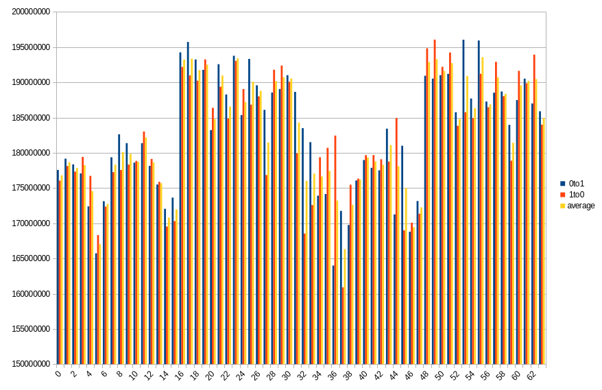
20.1 ℃, ~0 power off time, 36.06% changed bits
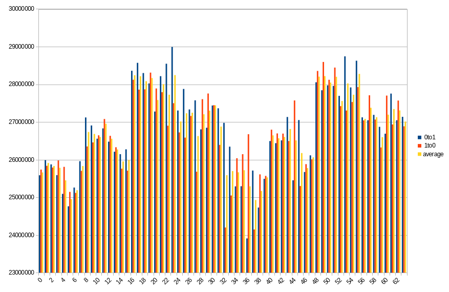
19.3 ℃, ~0 power off time, 39.28% changed bits
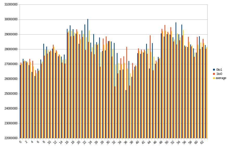
19.4 ℃, ~0 power off time, 41.04% changed bits
PC - DDR4 DIMM
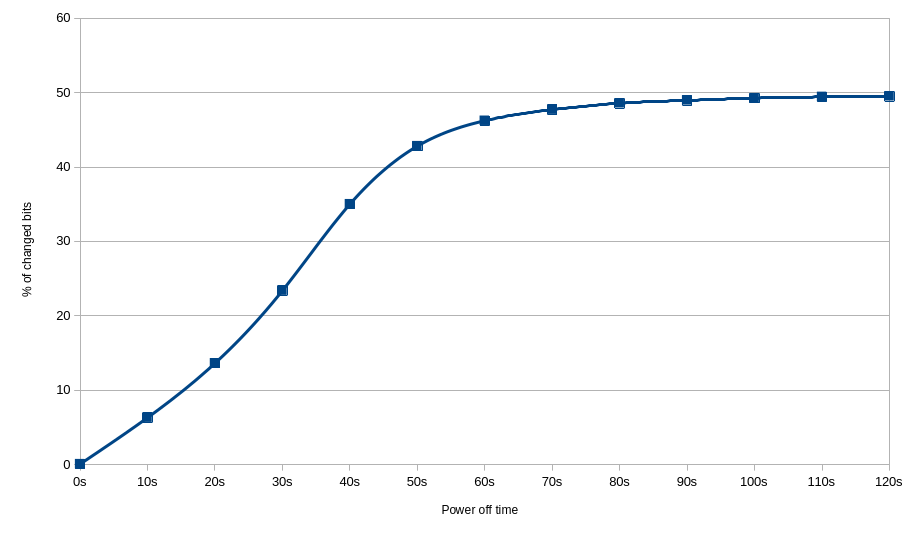
This platform showed much higher data preservation rates. We’ve been measuring at intervals of 10 seconds, starting from immediate power back, up to 2 minutes.
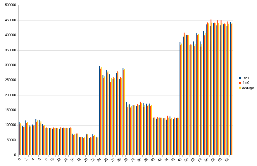
19.8 ℃, ~0 power off time, 0.08% changed bits
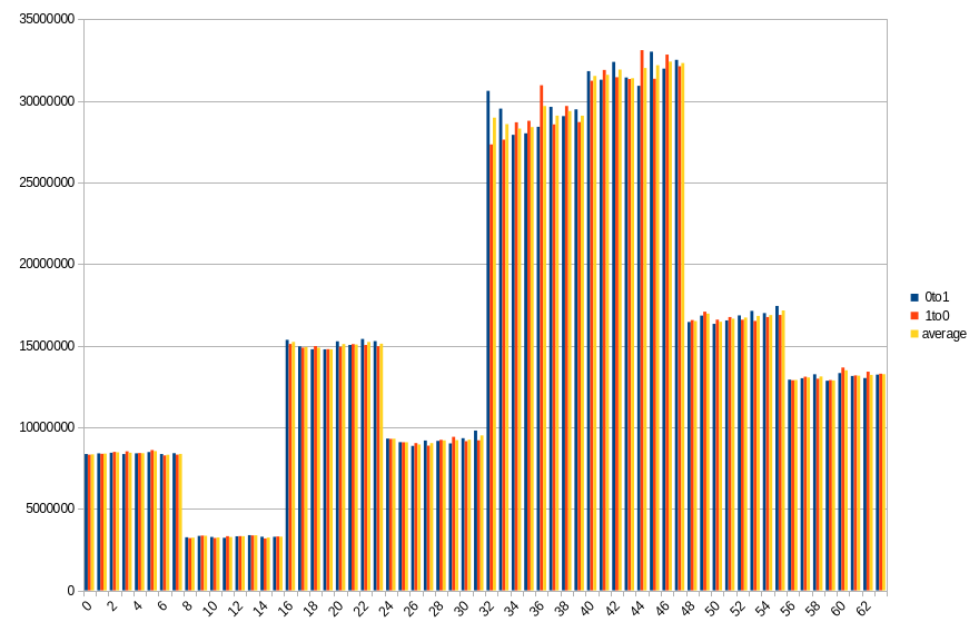
19.5 ℃, 10s power off time, 6.32% changed bits
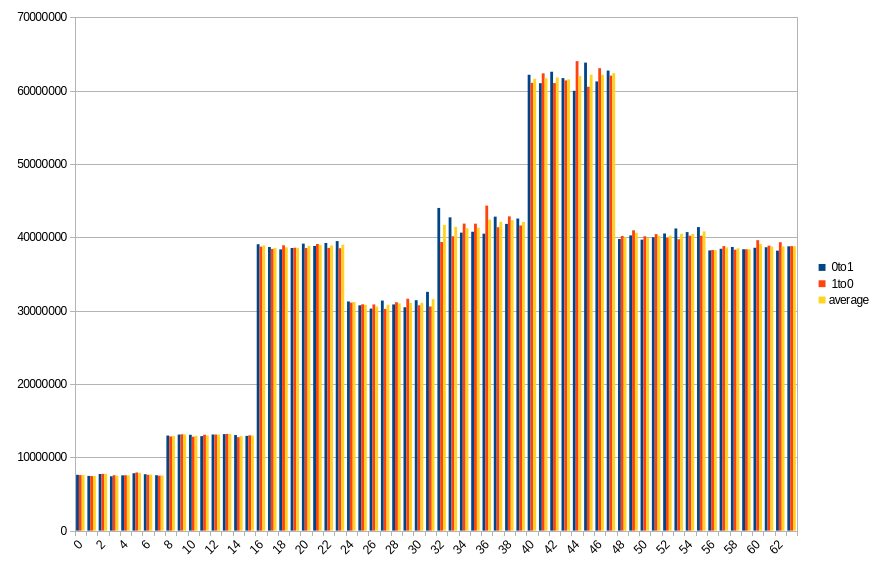
19.4 ℃, 20s power off time, 13.63% changed bits
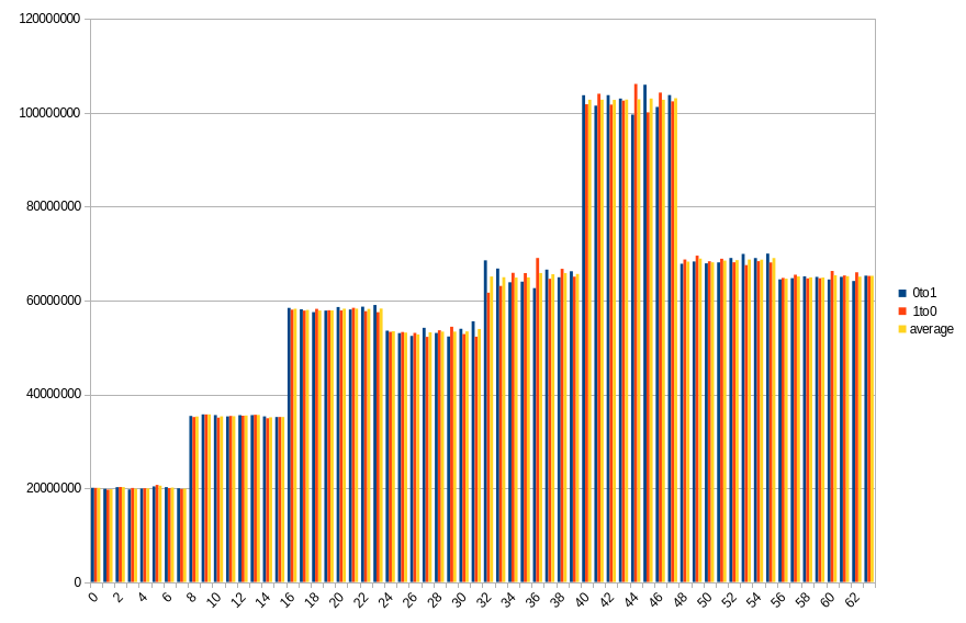
19.4 ℃, 30s power off time, 23.39% changed bits
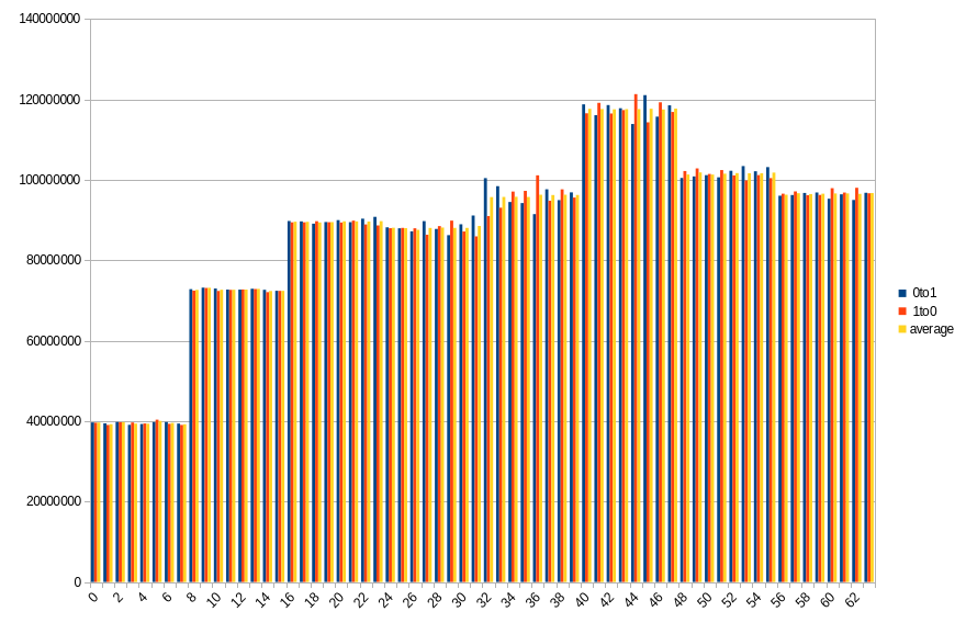
19.3 ℃, 40s power off time, 35.01% changed bits
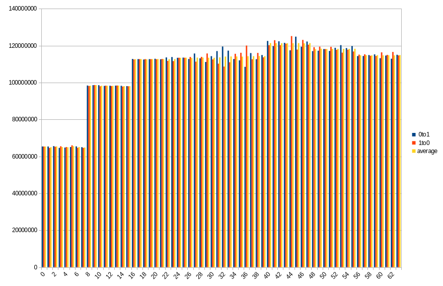
19.4 ℃, 50s power off time, 42.81% changed bits
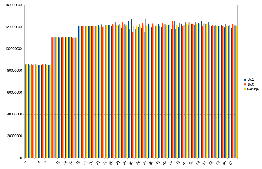
19.3 ℃, 60s power off time, 46.22% changed bits
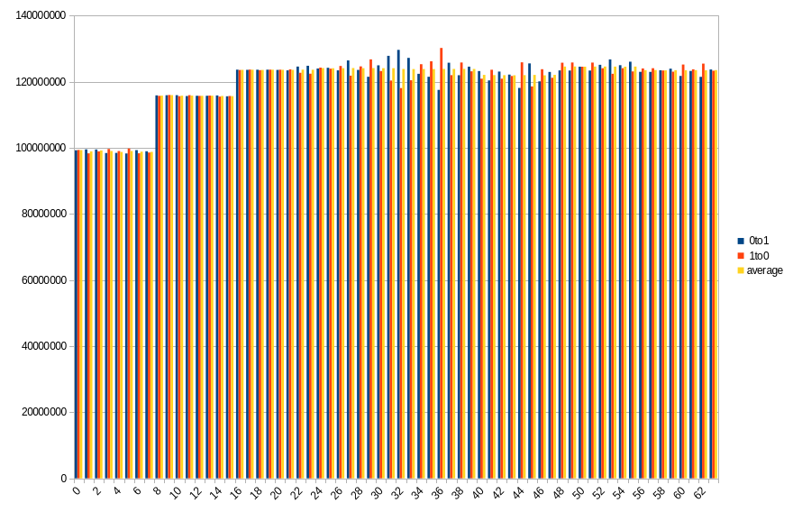
19.3 ℃, 70s power off time, 47.71% changed bits
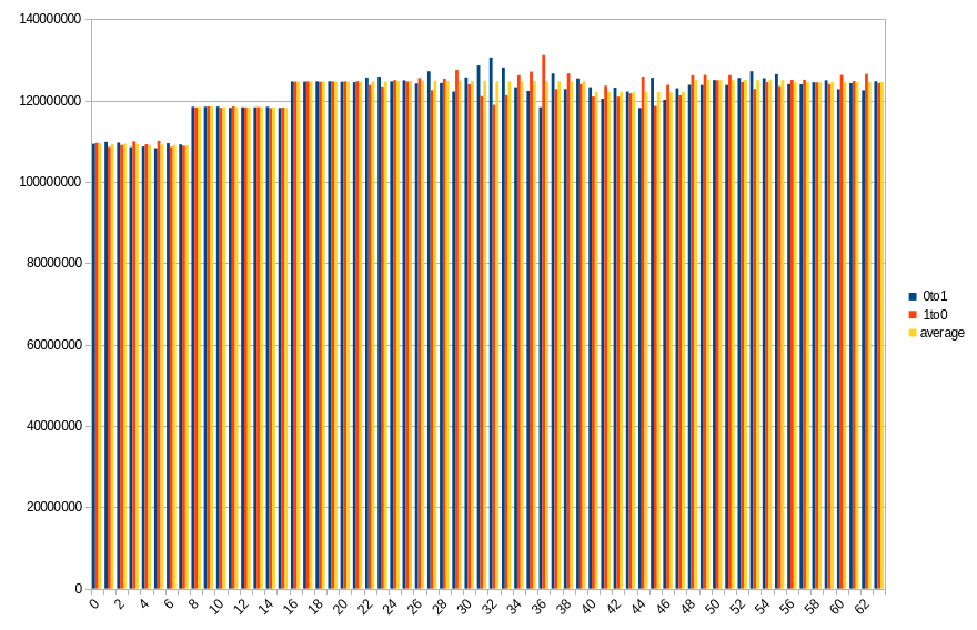
19.2 ℃, 80s power off time, 48.57% changed bits
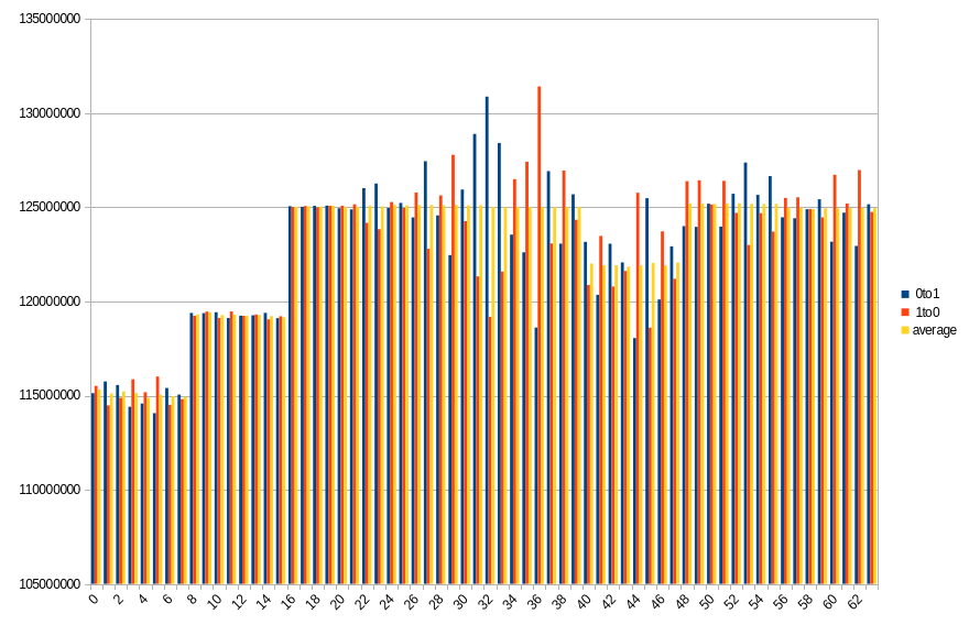
19.2 ℃, 90s power off time, 48.96% changed bits
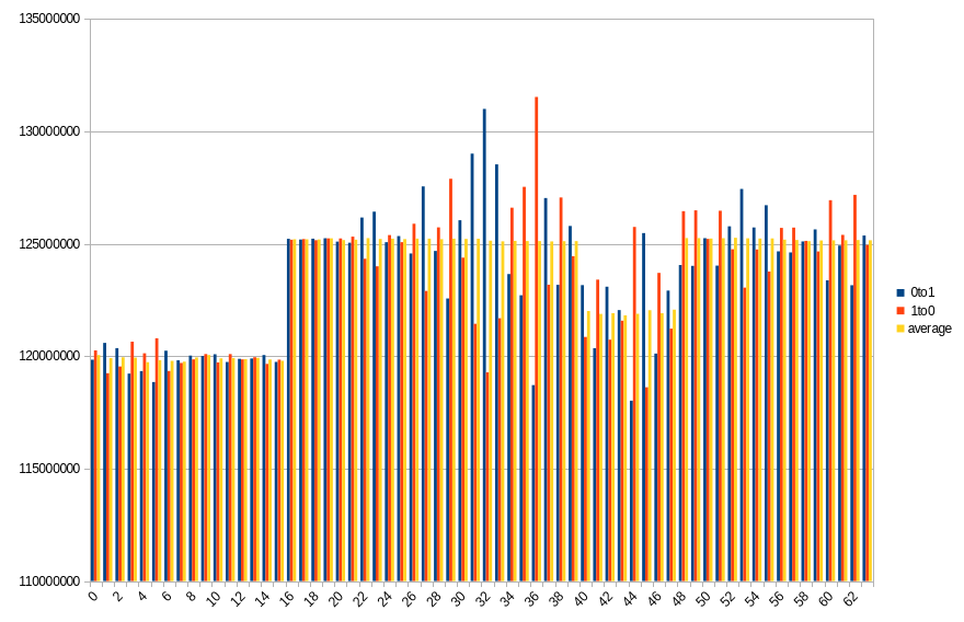
19.2 ℃, 100s power off time, 49.26% changed bits

19.1 ℃, 110s power off time, 49.43% changed bits
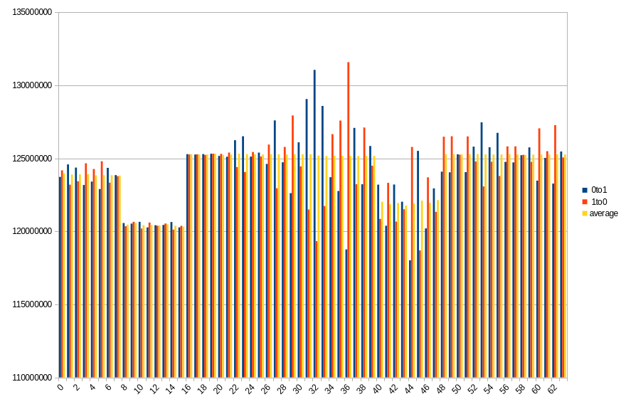
19.2 ℃, 120s power off time, 49.51% changed bits
With these measurement points, it was possible to construct a chart of preserved bits depending on power off time:
Conclusions
Both platforms show that the data decays with time, but the rate is significantly different between tested platforms. What took less than a second on DDR5 laptop, wasn’t achieved even after two minutes on DDR4 desktop.
On both platforms, impact of DIMM topology can be seen. In case of DDR5 SODIMM, distribution of changes in bits 0-31 roughly aligns with bits 32-63, especially with average values. Lower half has more 0 to 1 transitions, which in higher half is mirrored by 1 to 0 transitions. Border between DRAMs is also visible, although it isn’t that clear, contrary to DDR4 DIMM. Results from the latter show a clear difference between groups of 8 consecutive bits, with average almost constant within the group.
During a given run, some DRAMs start losing their data faster than others. It looks like this isn’t necessarily correlated with their maximal preservation time - take a look at group of bits 40-47 in DDR4. For delays in range 10-50 seconds, it is always the one that loses the biggest part of its content, but after that, it doesn’t get worse as fast as other groups do.
For DDR4, chart of percentage of lost bits in function of time shows that the amount of lost data rises quickly with lower delays, but then starts to slow down when it gets close to 50%. The plot is also flattened on the left side, which may suggest that some constant, systematic error is added to time measurements. In fact, after applying back the power, it takes about 5 seconds before power LED gets lit on that platform.
Summary
We’ve learned that RAM needs time to lose its content, and that this time varies between both tested configurations. Unfortunately, we don’t have enough data points to say what causes such difference. We would like to extend this research to include more platforms and different DIMMs in the future, if you’re interested in such content, let us know.
This research has been supported by Power Up Privacy, a privacy advocacy group that seeks to supercharge privacy projects with resources so they can complete their mission of making our world a better place.
Unlock the full potential of your hardware and secure your firmware with the
experts at 3mdeb! If you’re looking to boost your product’s performance and
protect it from potential security threats, our team is here to help.
Schedule a call with us
or drop us an email at contact<at>3mdeb<dot>com to start unlocking the hidden
benefits of your hardware. And if you want to stay up-to-date on all things
firmware security and optimization, be sure to sign up for our newsletter:
