The Hardkernel ODROID-H4 PLUS is available as part of the Dasharo Pro Package. Subscribe to the Dasharo Pro Package to access exclusive pre-built binaries. For added convenience, you can also purchase a platform with a subscription directly from our shop. As a subscriber, you will receive access to all firmware updates for the duration of your subscription via the Dasharo Pro Package newsletter, and gain entry to the Dasharo Premier Support invite-only live chat on the Matrix network, enabling direct engagement with the Dasharo Team and fellow subscribers for personalized, priority assistance.
Introduction
We recently stumbled upon this interesting piece of hardware from Hardkernel, the ODROID H4+. It is a nice, compact , low-power board with Alder Lake-N SoC. But that is not what makes it outrageous. In the hardware and firmware world, having public schematics is a rarity, almost non-existent, but this board actually has one! Yes! Imagine what a firmware developer thinks seeing this… Of course, it’s nothing else than an open-source firmware port. In this blog post, I would like to show you the perspective of firmware porting from scratch, beginning with the starting steps and the necessary preparation work you should do each time you deal with new hardware. You may also read about our plans related to this board on ODROID forum thread and Dasharo Roadmap.
Unboxing
Unboxing is probably the most pleasant moment (except the final result of having the working open-source firmware build) of the whole process. Let’s unpack this little baby and see what we got…
The platform came to me with three small boxes.
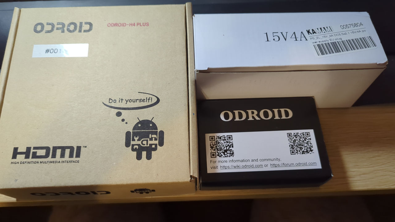
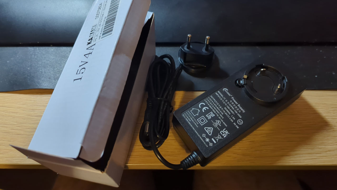
The white one has a power supply. It also has a switchable plug, which is useful when you travel and may need to switch the plug to other countries' standards.
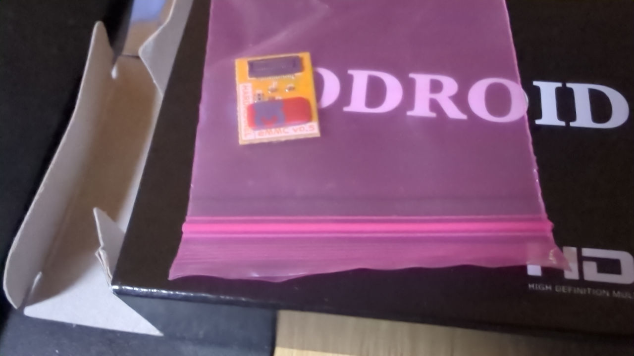
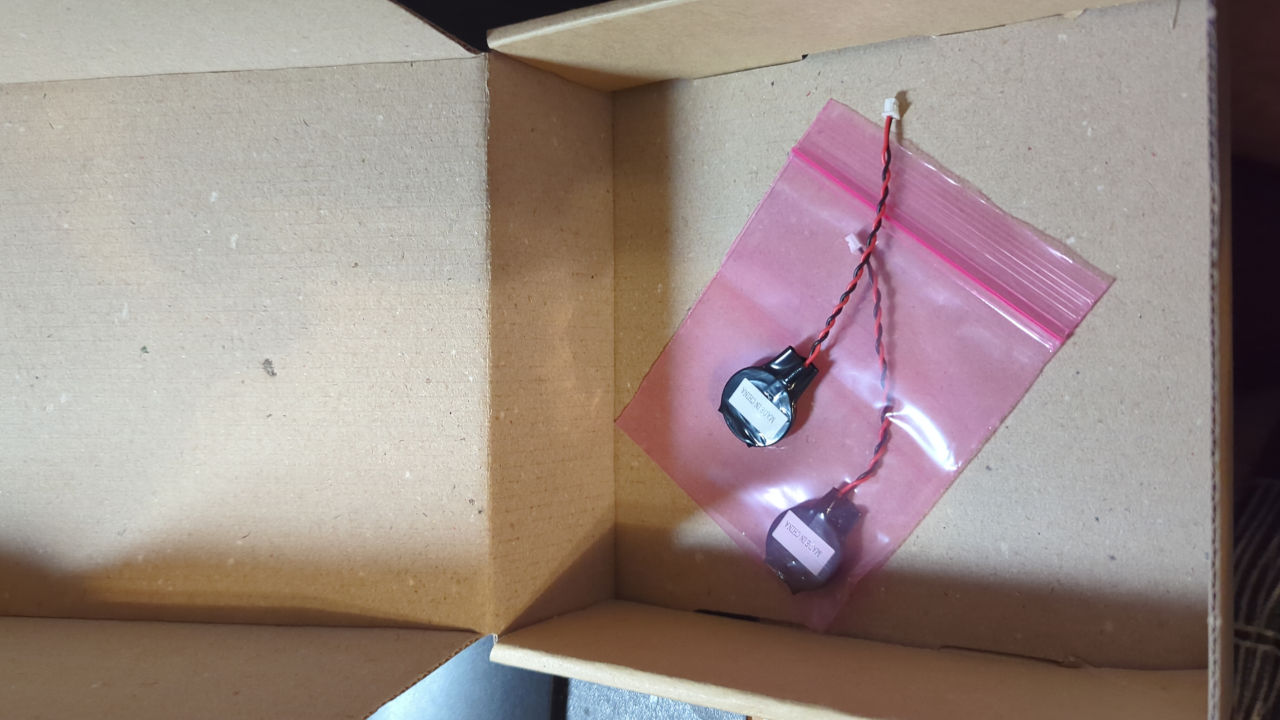
In the smaller dark box, there is a small bag containing an eMMC module with Hardkernel signature. Typically, you see eMMCs embedded on the board itself. However, the size constraints may have forced the designers to put it on a separate module or lower the board’s price. Cool, we will figure out how to connect it later.
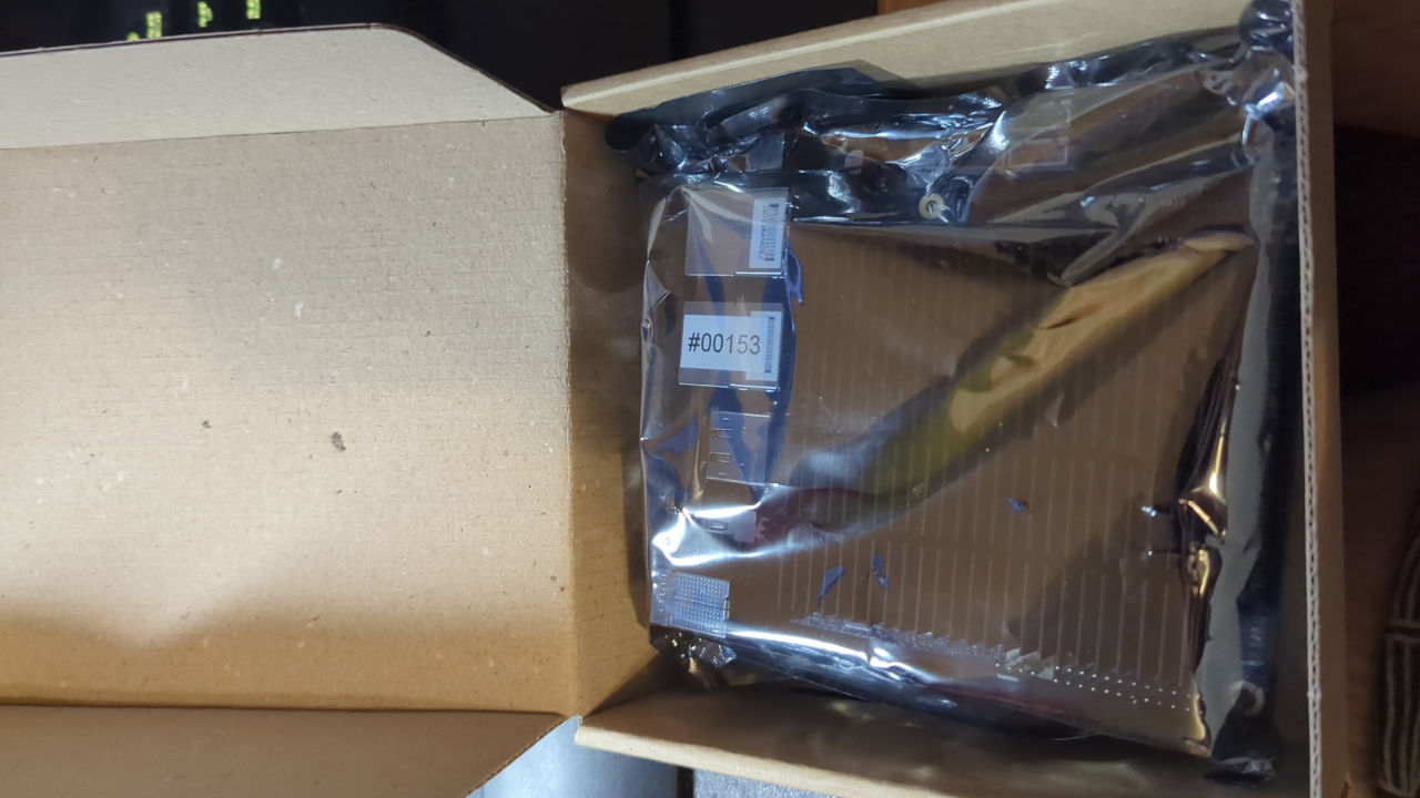
And now the shining start of our show. The board… It came packed in a electrostatic-proof bag.
Underneath it, we have two coin-cell batteries. As the Hardkernel page says:
BIOS Backup Battery (All H series models include a backup battery by default)
And they do include it, indeed.
The board itself is so tiny that it fits into my hand.
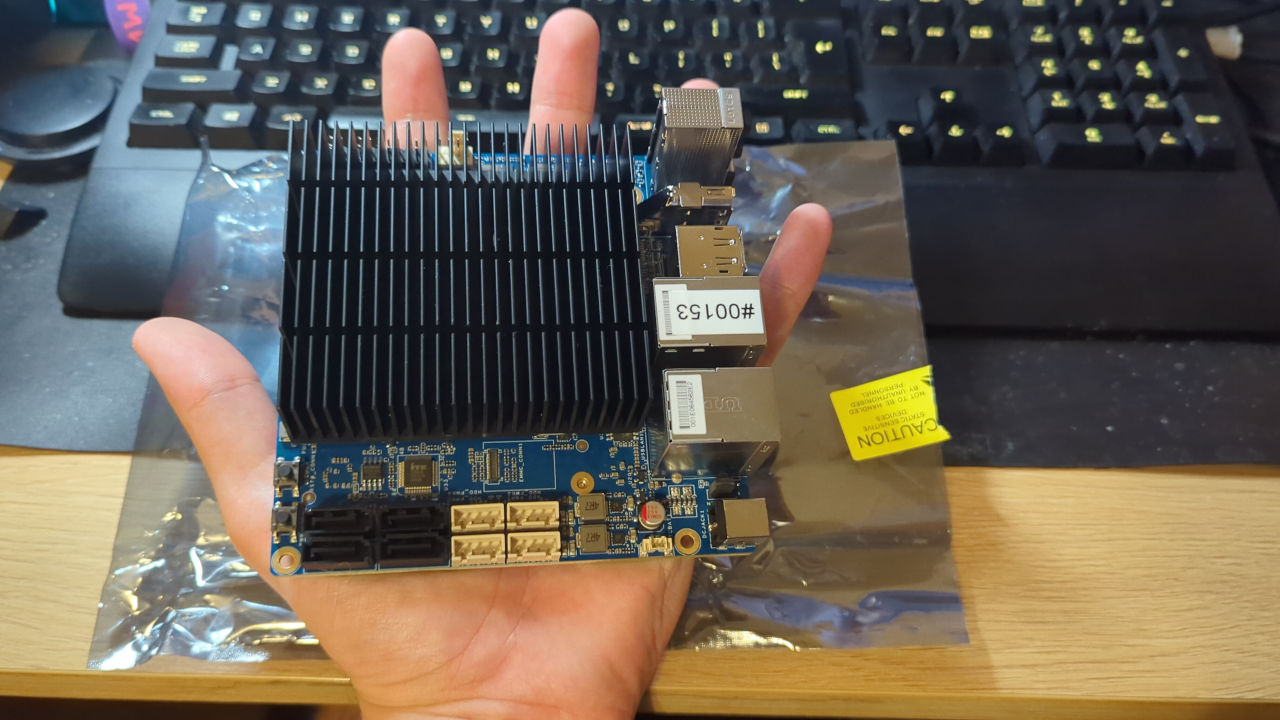
And mine already has a RAM stick plugged in. According to board specifications, it has single-channel DDR5 memory. In single channel configuration, it may reach a frequency of up to 4800MHz (also depending on the RAM stick of course).

First launch
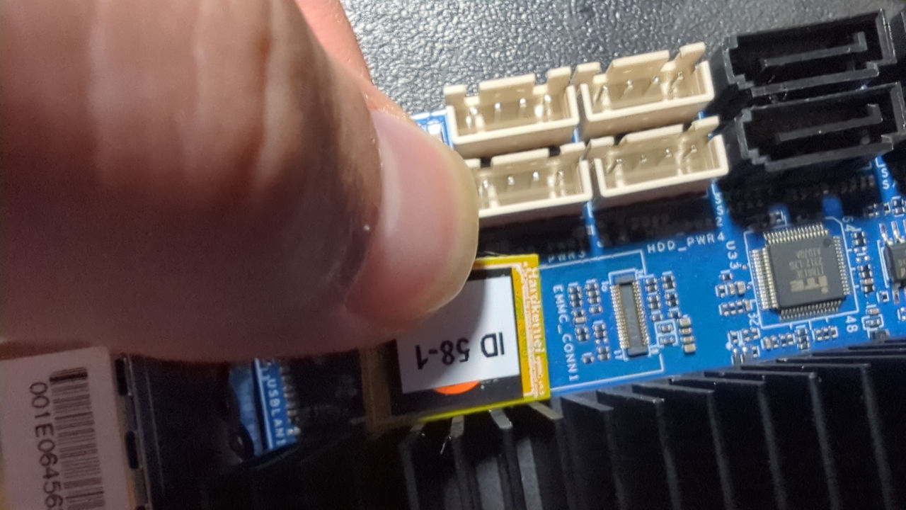
Before we attempt any work, let’s see if it even works… Things may happen during the shipping, so ensure it boots properly and there are no signs of damage before you start being rough with it. And believe me, we will (just a bit). Let’s plug one of the coin cell batteries so that our BIOS setting will not get reset every boot (typically, a CMOS battery reset will cause booting with default settings, like in last century PCs). Also, connect the eMMC module to check if the BIOS and OS detect it.
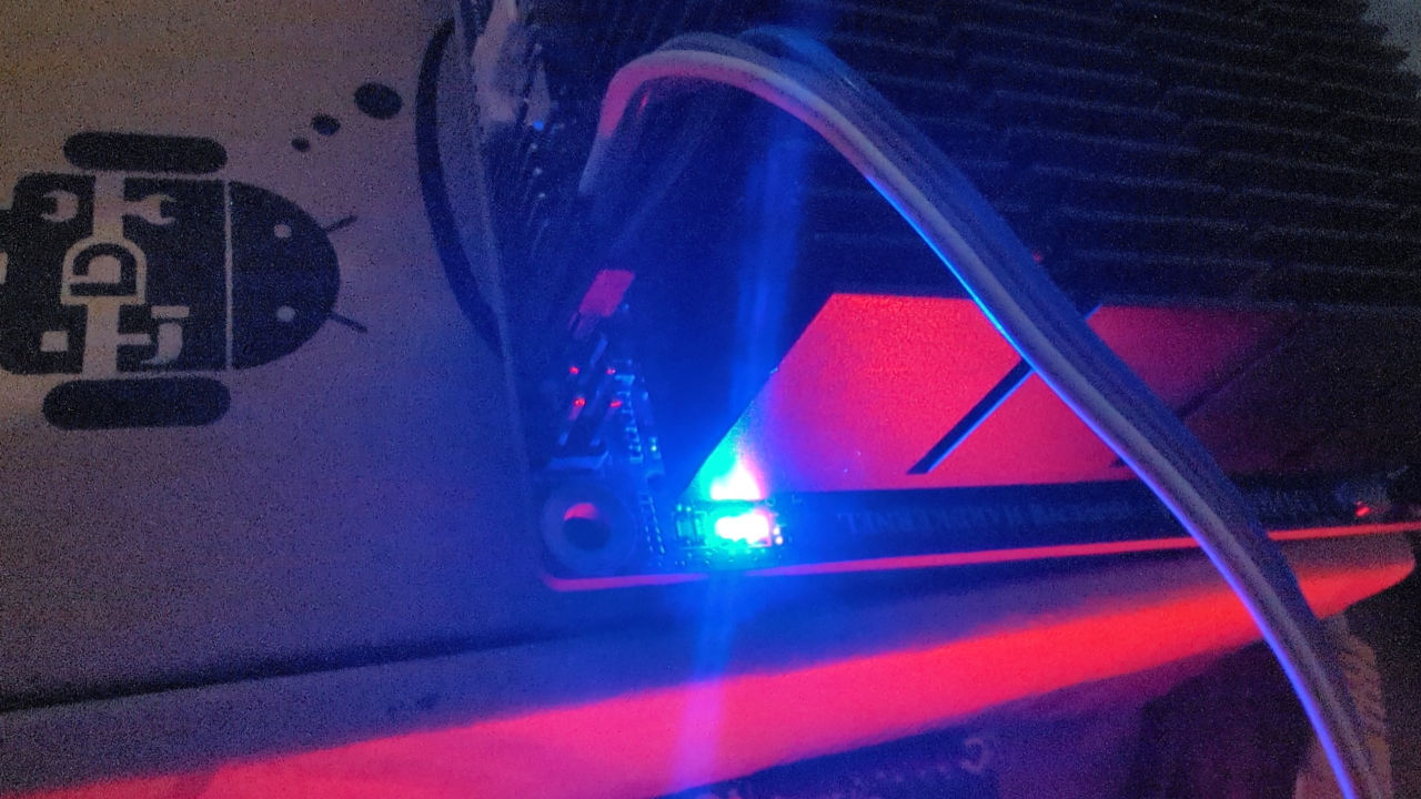
The first boot may take a few minutes and include board resets, so be patient. The board reset may be observed by the blue LEDs going off. When they are on, the board is booting/turned on:
After a while, you should be presented with a BIOS setup (assuming no bootable mediums were connected):
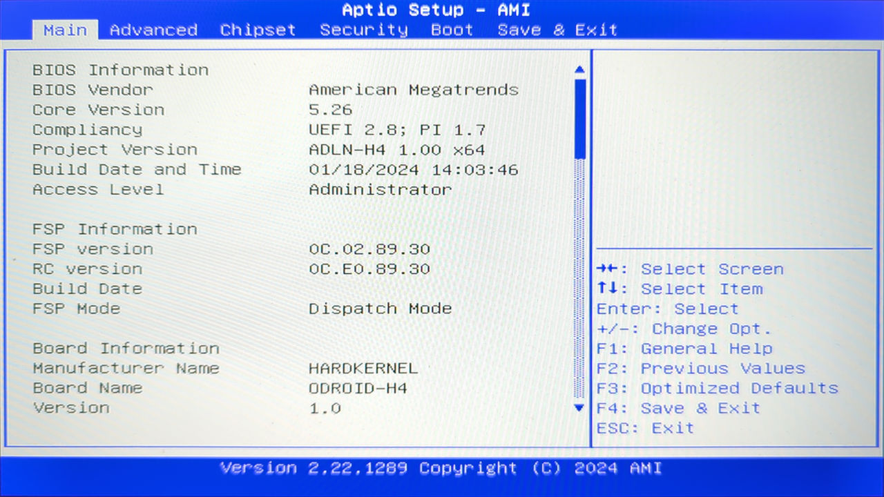
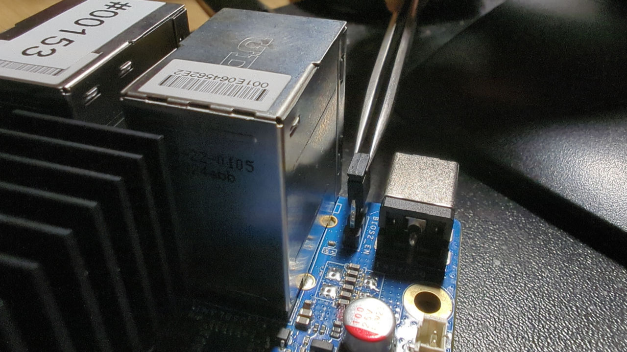
Apparently, this board has two BIOS SPI flashes switchable by a jumper. That is great! We don’t have to worry much about recovery; we can always switch to the flash with working firmware if something goes wrong. It will help a lot. Let’s switch the flash and boot it to see if there is valid firmware in the second flash chip. So let’s swap the jumper near the DC jack as the Hardkernel page says:
Dual BIOS: If the BIOS is corrupted due to a power outage during update, etc., you can boot into the backup BIOS and recover by moving the jumper next to the DC jack. This feature is only available on ODROID-H4+ and ODROID H4-Ultra.
Taking a dump (from the flash)
No, we are not going to the toilet… The time has come to take a dump of the SPI flash contents holding our BIOS. Remember, under any circumstances, do not try to overwrite your BIOS with some custom open-source firmware builds before you make a backup dump image of your current SPI flash contents and secure a recovery method (i.e., external flashing with a programmer).
We may take a dump using the flashrom on the board itself. It is the simplest and most reliable method. Still, it requires the chipset to be supported in flashrom (which may not always be the case, especially for the newest processors). For this purpose, we will use Dasharo Tools Suite (DTS) which already has the flashrom and is a small Linux distro we need to run this utility. So we quickly burn the image on the USB stick, connect the Ethernet cable to the board, boot DTS from the stick, enter the shell, and then:
|
|
Sometimes, the read may not succeed, e.g., if BIOS sets up read protection or
the flash descriptor does not permit reading certain regions. Then one must
specify the readable regions using --ifd -i <region1> -i <region2> ...
parameters to dump as much as possible. A complete dump is only possible with
an external programmer in such cases. Do a couple of dumps and check their
shasums, e.g., using sha256sum to ensure reliable reads.
|
|
For a good exercise, we will switch to the second flash, start the board again, and dump the second flash contents as well. And compare it to the first one. I did three more dumps:
|
|
The binary is not the same (it may result from different memory controller cached settings), but it does not matter much. Most importantly, shasums are consistent between dumps of the same flash chip.
Save one copy of the dump of each flash chip in a safe place in case you would need to flash it back. As a last resort, one may use the manufacturer’s BIOS binaries. Fortunately, Hardkernel provides those here, but this may not always be true for all manufacturers.
Dumping board and firmware information
While we are at dumping already, let’s extract all possible board information we need from the system. For this purpose, we will use the HCL report functionality integrated into the DTS. It already extracts information about the system, ACPI, SMBIOS, GPIOs, and other registers and structures that may prove helpful later. It also reads the complete flash for backup. Yes, we could go straight with HCL from the beginning, but for a better explanation, I decided to show the flashrom usage explicitly (not hidden behind some script). So, let’s go with it. We may do it either from the main DTS menu or the shell:
|
|
It may take a couple of minutes and results in a tarball with extracted logs and information:
|
|
Accessing flash with an external programmer
Before we can access the flash with an external programmer, we must determine a couple of things:
- What voltage does the flash operate with?
- What is the flash package, and do we have tools to hook onto it?
On the bottom side of the board, we notice two chips living near each other
marked as BIOS_SPI1 and BIOS_SPI2. Pretty obvious, isn’t it?
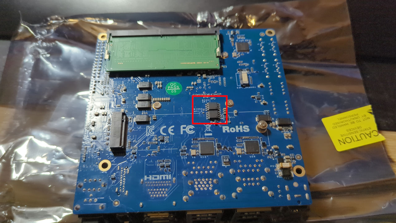
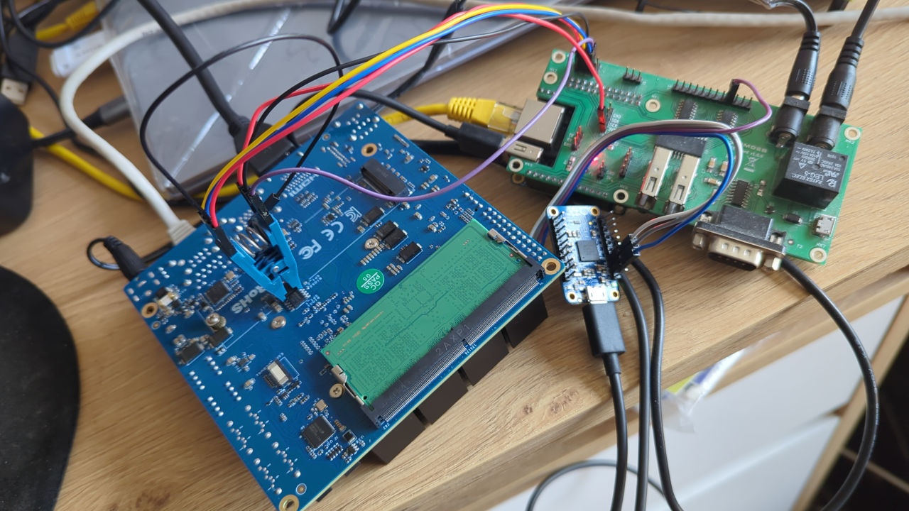
Thankfully, these are SOIC8 packages that can be hooked onto easily using a Pomona 5250 clip. Before we hook on it, we must check the chip name and search for a datasheet or specifications to verify the operating voltage. In this case, both chips are Winbond W25Q128JV, 128Mbit (16Mbyte) chips operating at 3V. So, a programmer with 3.3V will do perfectly fine here. One may also use the schematics to check what voltage rails are connected to the SPI chip, but these do not always give 100% certainty (I already saw schematics that were not actually reflecting the reality), and trust me, you don’t want to see smoke for such a stupid reason.
As a programmer, I will use the Remote Testing Environment (RTE) and connect the Pomona clip to the SPI header. For reference, every SPI flash SOIC8 chip has the same pinout:
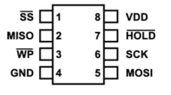
We have to connect the wires from Pomona pins (1:1 with the flash chip) to the RTE’s SPI header like this:
| Pomona/chip pin | RTE SPI header pin |
|---|---|
| 1 CS | 3 CS |
| 2 MISO | 5 MISO |
| 4 GND | 2 GND |
| 8 VDD | 1 VCC |
| 6 SCK | 4 SCLK |
| 5 MOSI | 6 MOSI |
Other pins do not have to be connected. Now, hook the Pomona on the first chip, matching the CS wire to the dot on the flash chip package, denoting the chip’s first pin. For more details with images, please visit Dasharo documentation.
Now invoke the flashrom command on RTE to check if the flash is detected by following the first three steps from this guide and then:
|
|
Do not pass -w with a parameter. We don’t want to flash yet.
If everything was connected correctly, flashrom should detect a chip. Some platforms may be tricky and require various conditions for the flash to be detected: platform powered on, platform powered off, platform cut off from power, platform held in reset state, etc. Try various scenarios and see which works for you. If you detected the flash chip, try to read it a couple of times and check the shasums as before to ensure the programmer’s reliability. If all shasums are the same, try to write the dump made earlier to confirm the flash write also works. Boot the platform after you flash the platform with an external programmer to confirm the programmer works reliably. In this case, you are safe because there is always a second flash you may boot from. However, in most cases, there isn’t. So, if you can’t manage to flash it, then you are in a bit of trouble. You have to keep trying until you succeed.
Setting up hardware with RTE
We already have connected the SPI flash. For a fully remote development stand, which is our goal (you don’t want to be constantly present near the board and use your hands to turn the platform on or off or recover from brick), we still need to be able to manage the power of the board:
- Connect/disconnect the power supply. Ideally, with the RTE relay switch/
- Power on and off the board using an RTE GPIO connected to the power button signal on the board.
- Reset the board using an RTE GPIO connected to the reset button signal on sthe board.
Sometimes, the boards come with power/reset button headers with well-marked
pins. However, in our case, we have complete schematics. We can search for the
power/reset button signals and whether they are exposed on a pin header
besides the board’s physical power and reset buttons. The easiest way is to
search by board markings: the power button is marked as PWR_ON1 and the
reset button as RST#_CONN. And bingo. The buttons are on page 25.
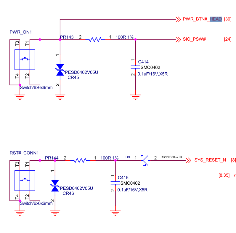
Now we know that we have to search for other occurrences of PWR_BTN#_HEAD
and SYS_RESET_N, which lead to our buttons. PWR_BTN#_HEAD can also be
found on the 24-pin expansion header on page 39, which is the pin we searched
for.
Good. However, the reset button is not available on any pin. That’s unfortunate. However, the power button is more important. As a last resource, one could solder a wire to the physical reset switch pad to get remote control of the reset button.
Now, we can connect the power button and the board’s power supply to RTE. Use the barrel jack of the power supply and plug it in one of the two barrel jack sockets on RTE (it doesn’t matter which one). Plug the one end of the male-to-male barrel jack cable to the other barrel jack socket on RTE and the second end to the board’s barrel jack socket.
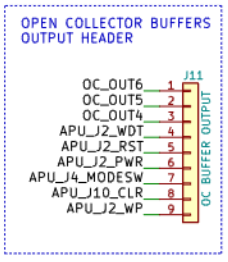
As for the power button, connect the board’s EXT_HEAD1 pin 17
(PWR_BTN#_HEAD) to the RTE GPIO header with OC buffers (J11) pin 6
(APU_J2_PWR). Note that the reset button and power button have predefined
pin locations on RTE J11 header (see RTE
schematics).
One last thing useful for development and testing is a serial port/UART. Not
all boards may have one. Even if there is a serial port, it is either not
exposed or hard to find without schematics or if the board’s headers are
poorly marked. Fortunately, ODROID H4+ has a serial port on the EXT_HEAD1
header: APU_UART0_RXD_BUF and APU_UART0_TXD_BUF. These are connected to
the ITE Super I/O serial port. We couldn’t wish for more. Connect it to RTE as
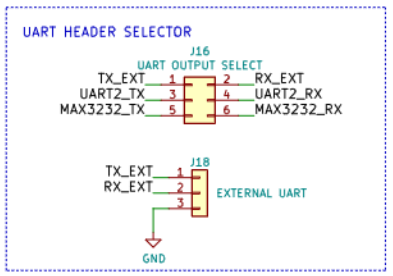
follows:
| ODROID H4+ EXT_HEAD1 | RTE J18 |
|---|---|
| 6 APU_UART0_RXD_BUF | 1 TX_EXT |
| 8 APU_UART0_TXD_BUF | 2 RX_EXT |
| 10 GND | 3 GND |
Additionally, put the jumpers on RTE J16 header into external UART mode (
short TX_EXT with UART2_TX and short RX_EXT with UART2_RX).
Note that Serial Console Redirection may be disabled in the BIOS, and you will not see anything on the serial port. In the case of ODROID H4+, it was not enabled by default, so you must explicitly enable it before checking if the serial console works. Also, disabling Quiet Boot may help (unless you want to spam the hotkeys to enter setup in blind). You may also find the generic testing stand setup instructions on Dasharo documentation.
Now, we are ready to test our remote development and testing setup. Try to turn the board on and off using the power supply and power button. Check if the board boots properly when the Pomona clip is hooked (by checking serial port output simultaneously) and if you can access the flash chip.
My setup used the RTE v0.5.3 hat (so connections would be slightly different, e.g., I had to use USB to UART converter for serial), and flashing worked while the PSU power was cut off with the relay. The board booted fine with Pomona hooked, which is ideal. Power on requires switching the relay state to connect the PSU to the board and sending a short pulse signal on the power button pin with RTE to get the board POST. Reading flash was also fine:
|
|
I took three dumps and did sha256sum. All good:
|
|
If everything works, you are ready to make the first steps in the coreboot firmware development. We will review the logs from HCL and schematics to note the most essential information for porting. But that’s a story for another day.
Summary
I hope you enjoyed reading the post (and possibly going through the process with me). If you love playing with hardware, are an open-source firmware enthusiast, and want to learn how to do firmware, 3mdeb may be a good place for you. Consider dropping us your CV.
The ODROID H4+ is a platform with huge potential for many other usages. It is a modern design with open schematics, utilizing a low power Intel N-series processor released in the first quarter of 2023. SPOILER: It may serve as a perfect target for training. Interested in polishing your skills? Be sure to be up to date with our training offer and activity on OST2. Here’s also a ODROID forum thread with our training plans.
You can also buy the ODROID H4+ with Dasharo firmware preinstalled directly from our store in two versions:
- Odroid H4 Plus with Dasharo (coreboot+UEFI) Pro Package for Network Appliance
- Training version used during OST2 workshops
Unlock the full potential of your hardware and secure your firmware with the
experts at 3mdeb! If you’re looking to boost your product’s performance and
protect it from potential security threats, our team is here to help. Schedule
a call with
us or
drop us an email at contact<at>3mdeb<dot>com to start unlocking the hidden
benefits of your hardware. And if you want to stay up-to-date on all things
firmware security and optimization, be sure to sign up for our newsletter: